Practical Throughput in PCIe Gen 1-4
PCIe Gen 4.0 is often stated to support 16 Gbps per lane, with a lane being defined as a pair of wires that allow for simultaneous data transmission and reception. Therefore, a PCIe connection with four lanes can theoretically achieve a total speed of 64 Gbps. However actual data rates on real devices will never reach this speed due to various factors. These include overhead from bit encoding, Transaction Layer Packet (TLP) and Data Link Layer Packet (DLLP) communications, and Physical Layer Packet (PLP) management. These protocols and encoding mechanisms consume signaling bandwidth, reducing the effective throughput available for data transfer. Additionally, practical throughput is further impacted by system-level latencies, such as operating system overhead, interrupt processing delays, and other software-related factors that affect overall data transfer efficiency beyond hardware-level protocol overheads.
Let's explore how these factors influence throughput across different PCIe generations.
Encoding Overhead
In PCIe, data is transmitted using specific encoding schemes that add extra bits to the data to ensure integrity and manage error detection. This encoding introduces an overhead, which impacts the effective data transfer rate.
PCIe Gen 1 and Gen 2 use 8B/10B encoding scheme, where each byte of data is converted into a 10-bit data code, resulting in a 25% encoding overhead.
PCIe Gen 3 and Gen 4 utilize a more efficient 128B/130B encoding scheme. Here, every 128 bits of data are encoded into 130 bits. This newer encoding method reduces the encoding overhead significantly to about 1.5%.
TLP Overhead
A Transaction Layer Packet (TLP) in PCIe is a fundamental data structure used for communication between devices. TLPs encapsulate the data payload and include various control information necessary for ensuring proper data transfer, error detection, and flow control within the PCIe architecture. Each TLP consists of a header, which specifies the transaction type (such as memory read/write or I/O read/write), an optional data payload, a Link CRC (LCRC) for error checking and an optional end-to-end CRC (ECRC) to enhance error checking and recovery.
TLP can vary in size depending on the transaction, typically ranging from 12 to 16 bytes, and may include optional fields such as ECRC.
| Start | Sequence ID | TLP Header | Data Payload | ECRC | LCRC | End |
| 1 byte | 2 bytes | 12-16 bytes | 0-4096 bytes | 4 bytes | 4 bytes | 1 byte |
The overhead includes the following fields:
- Start and End framing symbols (2 bytes)
- Sequence ID (2 bytes)
- TLP header (12-16 bytes)
- ECRC (4 bytes)
- LCRC (4 bytes)
The PCIe specification permits a maximum payload size of 4096 bytes in theory, but in practice, such large buffers are rarely used due to compatibility and latency concerns. Our PCIe Gen 4 implementation allows up to 1024-byte payloads. Additionally, in most systems, testing has shown that the payload size is often limited to much smaller values (most motherboards use between 128 and 512 bytes) due to constraints imposed by the motherboard chipset, PCIe switches, or endpoints with limited buffer capacities.
TLP Overhead Impact on Throughput
Considering the overhead in packets for write operations, the total overhead will be 28 bytes. This means for a 256-byte maximum payload size, the maximum possible throughput is (256 / (256 + 28)), or 90%.
The following figures show the maximum theoretical throughput possible for Gen 4 and Gen 2 slots with different TLP header sizes, including encoding overhead but excluding any DLLPs, PLPs, and OS-related latencies. Note that Gen 3 speeds are roughly half of Gen 4 speeds, and Gen 1 speeds are about half of Gen 2 speeds, due to the use of the same encoding schemes within these generation pairs.
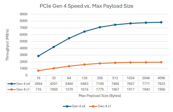
Note: TLP Header size is 16 bytes and includes ECRC.
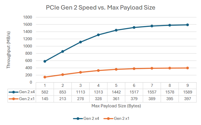
Note: TLP Header size is 16 bytes and includes ECRC.
Other Overheads
In addition to encoding and TLP overheads, several other factors can further impact PCIe performance. For PCIe Gen 4, it's advisable to account for an additional 250MB of bandwidth reduction due to various overheads and latencies, including:
- Link Layer Overheads: This includes flow control and acknowledgment packets.
- Interrupt Latency: Delays between the generation and handling of interrupts, which can affect how quickly PCIe events are processed by the CPU.
- Additional Hardware: The presence of other devices connected to the root complex through PCIe switches can introduce additional latency and share bandwidth, potentially reducing available throughput.
- OS-Related Latencies: System-level delays caused by the operating system's management of I/O operations.
- CPU Utilization: High CPU load can impact PCIe performance by affecting the speed at which data is processed and transferred.
Practical PCIe Slot Speed Measurements
In this part of the analysis, we've tested the actual speeds of PCIe slots on various machines using our PCIe Gen4 test card to give you an idea of the performance you can expect.
| CPU | Motherboard | Operating System/Build Number | PCIe Link Configurations | Max Read/Write Speed (MB/s) |
| AMD Ryzen 9 3900 12-Core Processor | Gigabyte X570 AORUS MASTER | Windows 11 Professional Edition build 22631 (64-bit) | Max Link Speed: Gen 4 Link Speed: Gen 4 Link Width: x4 MPS: 512 bytes MRRS: 512 bytes |
6971/6764 |
| AMD Ryzen Threadripper 3970X 32-Core Processor | Gigabyte TRX40 AORUS XTREME | Windows 10 Home build 19045 (64-bit) | Max Link Speed: Gen 4 Link Speed: Gen 4 Link Width: x4 MPS: 512 bytes MRRS: 512 bytes |
6920/6746 |
| Intel(R) Core(TM) i5-14600K 3.50 GHz | Gigabyte Z790 UD AX | Windows 11 Professional Edition build 22631 (64-bit) | Max Link Speed: Gen 5 Link Speed: Gen 4 Link Width: x4 MPS: 256 bytes MRRS: 512 bytes |
6563/6368 |
| Intel i5-10400 | MSI MAG Z490 TOMAHAWK (MS-Z7c80) | Windows 10 Professional Edition build 19045 (64-bit) | Max Link Speed: Gen 3 Link Speed: Gen 3 Link Width: x4 MPS: 256 bytes MRRS: 512 bytes |
3267/3297 |
| Intel i3-12100 | ASUS Prime Z690-A | Windows 11 Professional Edition build 22621 (64-bit) | Max Link Speed: Gen 3 Link Speed: Gen 3 Link Width: x4 MPS: 256 bytes MRRS: 512 bytes |
3297/3384 |
MPS: Max Payload Size, MRRS: Max Read Request Size
Please note for PCIe Gen 5 and higher slots, while our card can still operate, the speeds will be restricted to PCIe Gen 4 levels.